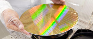
SEPAREL® Degassing for Semiconductors
Control Fluid Degasification and Aeration in Semiconductor Microchip Processing Using SEPAREL® Hollow-Fiber Membrane Degassing Modules
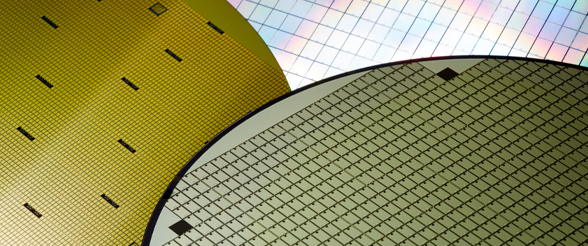
SEPAREL® membrane degassing technology can be used in a wide range of applications in the front-end processes of semiconductor chip processing. Providing excellent degassing for plating solutions, photoresist immersion lithography, etching, and developing solution.
SEPAREL® membrane degassing technology is manufactured to semiconductor standards at DIC Corporation’s facility in Chiba, Japan. All products are tested and inspected as required by semiconductor standards.
Major Applications
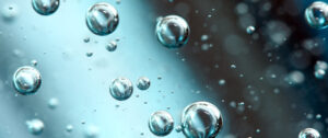
- Wafer cleaning; aeration for functional water production
- Deposition process; degassing plating solutions
- Photoresist coating; Degassing photoresist
- Exposure; degassing immersion liquid
- Development; degassing developer solution
- Etching; degassing etching solution
Resources
Learn more about the SEPAREL Membrane Degassing options for your application
Contact usRelated products
-
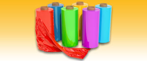
SEPAREL® Membrane Degassing for Films and Coatings
Read more -
SEPAREL® Membrane Degassing Technology and eFlow®Anti-Static Device
Read more -

SEPAREL® Membrane Degassing for Analytical Devices
Read more -
Membrane Water Degasification Technology
Read more -

SEPAREL® Membrane Degasification Technology for Inks
Read more